Digital to Analog Converter : DAC 0800
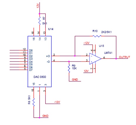
Digital to Analog Converter(DAC 0800) with Current to Voltage converter(LM741)
In electronics, a digital-to-analog converter (DAC or D-to-A) is a device for converting a digital (usually binary) code to an analog signal (current, voltage or electric charge). Digital-to-analog converters are interfaces between the abstract digital world and analog real life. An analog-to-digital converter (ADC) performs the reverse operation.
A DAC usually only deals with pulse-code modulation (PCM)-encoded signals. The job of converting various compressed forms of signals into PCM is left to codecs.
Basic Operation:
The DAC fundamentally converts finite-precision numbers (usually fixed-point binary numbers) into a physical quantity, usually an electrical voltage.
Normally the output voltage is a linear function of the input number. Usually these numbers are updated at uniform sampling intervals and can be thought of as numbers obtained from a sampling process. These numbers are written to the DAC, sometimes along with a clock signal that causes each number to be latched in sequence, at which time the DAC output voltage changes rapidly from the previous value to the value represented by the currently latched number. The effect of this is that the output voltage is held in time at the current value until the next input number is latched resulting in a piecewise constant output. This is equivalently a zero-order hold operation and has an effect on the frequency response of the reconstructed signal.
Basic Operation:
The DAC fundamentally converts finite-precision numbers (usually fixed-point binary numbers) into a physical quantity, usually an electrical voltage. Normally the output voltage is a linear function of the input number. Usually these numbers are updated at uniform sampling intervals and can be thought of as numbers obtained from a sampling process. These numbers are written to the DAC, sometimes along with a clock signal that causes each number to be latched in sequence, at which time the DAC output voltage changes rapidly from the previous value to the value represented by the currently latched number. The effect of this is that the output voltage is held in time at the current value until the next input number is latched resulting in a piecewise constant output. This is equivalently a zero-order hold operation and has an effect on the frequency response of the reconstructed signal.
The fact that practical DACs do not output a sequence of dirac impulses (that, if ideally low-pass filtered, result in the original signal before sampling) but instead output a sequence of piecewise constant values or rectangular pulses, means that there is an inherent effect of the zero-order hold on the effective frequency response of the DAC resulting in a mild roll-off of gain at the higher frequencies (a 3.9224 Db loss at the Nyquist frequency).
This zero-order hold effect is a consequence of the hold action of the DAC and is not due to the sample and hold that might precede a conventional analog to digital converter as is often misunderstood.
DAC0800
The DAC0800 series are monolithic 8 bit high speed current output digital to analog faturing typical setting times of 100ns. When used as a multiplying DAC, monotonic performance over a 40 to 1 refeence current range is possible. The DAC0800 series also features high complemementary current output to allow diferential output voltages of 20 Vp-p with simple resistor loads. The reference to full scale current matching of better than l LAB elimanates the need for full scale trims in most application while the nonlinearities of better than 0.1 over temperature minimize system error accumulations.
The noise immune inputs of the DAC0800 series wil accepet TTL levels with the logic thershold pin grounded. Channging the Vlc potential will allow direct interface to other logic families. The pefrormance and characteriststics of the device are essentially unchanged over the full 4.5v to 18v power supply range power dissipation is only 33mvw with +5v supplies and is independent of the logic input states.
The output of the DAC is current signal. So it is given to current voltage converter which is constructed by the LM 741 operational amplifier. Finally the anlaog voltage is given to Triac or SCR control circuit.


2 comments:
thanks for the blog. this is a nice blog with clear diagrametic representation
thank you
projects for it chennai
Hi,
Thank you for posting this blog with the circuit schematics.
I was curious about R10 specified as 2k2/5k1; is this meant to be read as 2k2 in parallel with 5k1, or is the value for Rf either 2k2 OR 5k1, depending on the load to be driven by the Op Amp?
Why is the Op Amp's output voltage asymmetrical? I measured the analog voltage when the binary input 0000 0000 (base 2) is applied at +2V72 (+2.72V), the close to zero volts value of +0V01 at the binary input of 0001 1100 (base 2) or decimal value of 28, and the value corresponding to binary input 1111 1111 (base 2) of -8V70.
Post a Comment